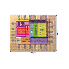
Design of mixed-signal CMOS-integrated sensor interface circuits
Summary
Continuous-Time Sigma-Delta ADCs (Analog-to-Digital Converters) are a specialized type of ADC that excel in converting analog signals into their digital form with high precision and low noise. Unlike discrete-time counterparts, continuous-time Sigma-Delta ADCs integrate the input signal continuously over time, allowing them to handle higher frequencies. Also, they don’t require additional anti-aliasing filters. These converters are particularly well-suited for applications requiring direct interfacing with sensors, such as photodiodes, because they can efficiently process both voltage and current signals. Continuous-time Sigma-Delta ADCs are known for achieving high resolution and dynamic range while maintaining low power consumption, making them ideal for use in compact, battery-powered devices. Their design enables significant chip miniaturization, a critical advantage in developing next-generation quantum sensors and other advanced technologies that require precise and efficient analog-to-digital conversion.
Content
In this project, you will design an analog circuit (operational amplifier plus additional circuitry) on the transistor level in the Cadence Virtuoso design environment. You will perform simulations to verify the performance of the circuit. The design goal is a low-noise current sensing Sigma-Delta Analog-to-Digital Converter, which could be used to create state-of-the-art sensor frontends.
Your tasks
- Short introduction to Sigma-Delta Analog-to-Digital Converters
- Specification of the required building blocks and top-level simulation with ideal models
- Transistor level design of CMOS amplifiers (OTAs) and simulation
- Design of high-speed CMOS comparators
- Verification of the designed building blocks in a top-level testbench
What we provide
Access to state-of-the-art design tools and the possibility to gain hands-on experience with chip integrated Analog-to-Digital Converter design
Requirements
- Attended lecture „Circuit Design in Nanometer-Scaled CMOS” is mandatory
- Alternatively, attending other lectures on CMOS-amplifier design will be considered for the requirement
Organization
- Contact: M.Sc. Philipp Hengel
- Module description, content, dates and registration can be found on C@mpus
- Documents on ILIAS
Contact

Jens Anders
Prof. Dr.Institute Director


